Potential Barrier In Pn Junction Diagram
Potential barrier junction pn using voltage contact electrical explain why measuring voltmeter electronics cannot measured companion someone above please book Junction potential barrier connected Junction pn barrier operation formation diodes basic electronics
semiconductor physics - Extremely forward biased pn junction - Physics
Barrier potential junction depletion region diagram explain formation help pn positive diode cycle half class physics corresponding conducts working does Potential barrier junction Forward biased junction pn potential barrier semiconductor height extremely led reduced physics
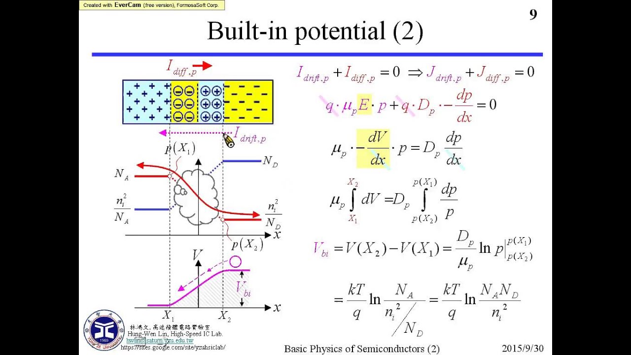
第三周之3 calculation of built in potential of pn junction
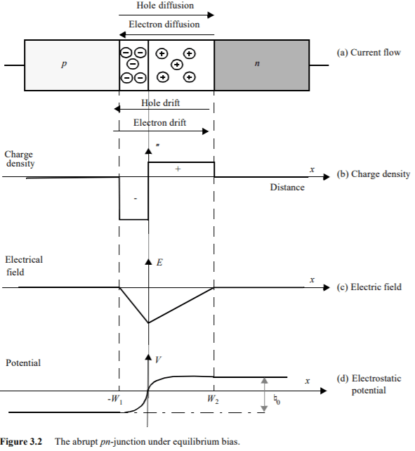
Junction pn diode field electric potential across charge density under equilibrium plot plots electrical axis horizontalWhat is pn junction Junction energy bias field biased potential electrostatic transition region electric effectsIn figure, v0 is the potential barrier across a p-n junction, when no.
Semiconductor physicsWhat is pn junction Pn junction operationPotential built junction pn calculation.
![Explain with the help of a diagram the formation of depletion region](https://i2.wp.com/ask.learncbse.in/uploads/db3785/original/2X/1/15b94645e4ead72cc461606cdc4d1378a4fd984f.png)
Junction depletion barrier valence conduction
Semiconductor physicsElectric field and potential plots across a pn junction diode Barrier potentialExplain with the help of a diagram the formation of depletion region.
Junction pn barrier depletion diode discussRegion charge space depletion stack why junction pn exchange Explain the formation of potential barrier in a p19. pn-junction — modern lab experiments documentation.
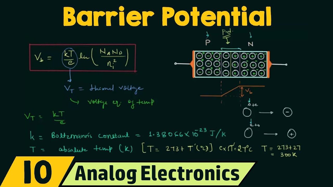
![What is PN Junction - The Engineering Knowledge](https://i2.wp.com/www.theengineeringknowledge.com/wp-content/uploads/2019/12/At-the-instant-of-junction-formation.jpg)
Potential barrier
.
.
![9/10/01 clc](https://i2.wp.com/www.phys.ksu.edu/personal/cocke/classes/phys506/spectra_files/image007.gif)
![19. PN-Junction — Modern Lab Experiments documentation](https://i2.wp.com/wanda.fiu.edu/boeglinw/courses/Modern_lab_manual3/_images/pn-junction_energy.png)
![What is PN Junction - The Engineering Knowledge](https://i2.wp.com/www.theengineeringknowledge.com/wp-content/uploads/2019/12/Formation-of-the-Depletion-Region.jpg)
![semiconductor physics - Why does the space charge in the depletion](https://i2.wp.com/i.stack.imgur.com/MccNc.png)
![semiconductor physics - Extremely forward biased pn junction - Physics](https://i2.wp.com/i.stack.imgur.com/Z4Xz9.jpg)
![第三周之3 Calculation of Built in Potential of PN Junction - YouTube](https://i.ytimg.com/vi/sZc33Ih-Q6o/maxresdefault.jpg)
![In figure, V0 is the potential barrier across a p-n junction, when no](https://i2.wp.com/cdn.tardigrade.in/img/question/physics/dc24a3fa5941be56c5ab4b3615023483-.png)
![voltage - Measuring barrier potential of a pn junction using a](https://i2.wp.com/i.stack.imgur.com/GMGSh.png)
![Barrier Potential - YouTube](https://i.ytimg.com/vi/itL2MQqZtqA/maxresdefault.jpg)
![Electric field and potential plots across a pn junction diode](https://i2.wp.com/i.stack.imgur.com/UQoN8.png)